








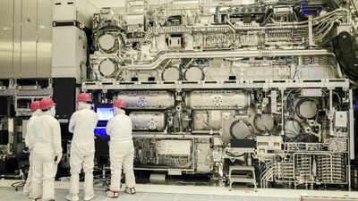
An ASML EUV scanner is not just a machine; it is a mechanical marvel widely regarded as the most complex industrial apparatus ever created by humanity.
Semiconductors — silicon chips measuring mere millimeters across — have become the most crucial technology in the modern world. They are the nerve centers of everything from smartphones and cloud-based Artificial Intelligence models to quantum computing nodes and hypersonic missile guidance networks.Because advanced computing power translates directly into economic dominance and military superiority, semiconductors are no longer treated as mere commodities.Instead, they are the subject of the tightest, most fiercely contested technological regulations in human history.At the apex of this global struggle lies a single, unfathomably complex manufacturing process: Extreme Ultraviolet (EUV) lithography.For years, Western policymakers rested easy under the assumption that China was permanently locked out of this frontier.
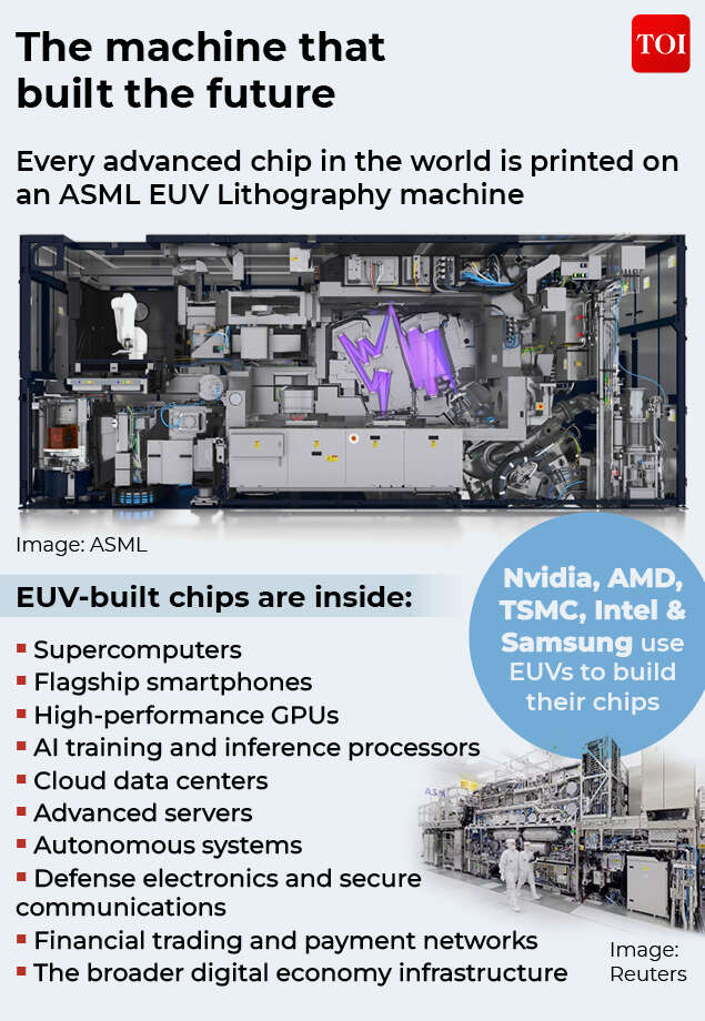
Semiconductors — silicon chips measuring mere millimeters across — have become the most crucial technology in the modern world.
However, stunning developments out of highly secure laboratories in Shenzhen suggest that Beijing may have just executed a technological insurgency, shaking the foundations of the global chip war.
The stuff of science fiction
To understand the scale of China’s alleged breakthrough, one must look to Veldhoven, a quiet town in the Netherlands.It is the home of ASML (Advanced Semiconductor Materials Lithography), the only company on Earth capable of designing and building EUV lithography systems.To understand why this machine is a bottleneck, one must appreciate the brutal physics of printing circuits at the atomic scale.
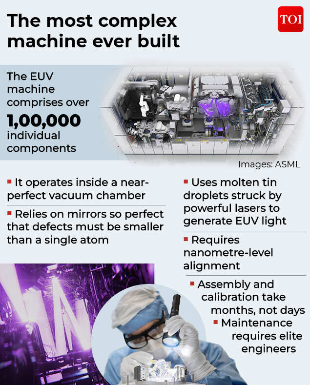
An ASML EUV scanner is not just a machine; it is a mechanical marvel.
Traditional chipmaking relies on Deep Ultraviolet (DUV) light, which operates at a wavelength of 193 nanometers (nm). While DUV can be pushed to its absolute physical limits using immersion techniques (flooding the space between the lens and the wafer with water), it eventually hits a wall.When features on a silicon wafer shrink below 7nm, trying to etch them with DUV light is akin to trying to draw a microscopic portrait with a thick Sharpie marker. The lines blur, the transistors bleed into one another, and the chip fails.EUV lithography solves this by radically dropping the light wavelength to 13.5 nm — clumping it tightly into the extreme ultraviolet spectrum, right on the border of X-rays.
Lights and mirrors
Generating a stable stream of 13.5 nm light requires a process that sounds like science fiction:
- A generator drops 50,000 microscopic molten tin droplets per second through a vacuum chamber.
- A high-power carbon dioxide laser fires a double pulse at each individual drop.
- The first pulse flattens the droplet; the second vaporises it into a plasma cloud reaching temperatures hotter than the surface of the sun.
- This exploding plasma emits the elusive 13.5 nm EUV light
EUV light is so volatile that it is absorbed by virtually everything, including standard optical glass and even the air we breathe.Therefore, the entire operation must take place within an ultra-high vacuum chamber.Instead of using standard lenses to focus the light, the system uses an array of specialised, atomic-level flat mirrors that take months to produce.These mirrors are coated with alternating layers of molybdenum and silicon, polished to an accuracy where the largest surface defect is no taller than a single atom.The light bounces off these mirrors, striking a photomask to transfer the circuit blueprint onto a silicon wafer coated with a light-sensitive chemical called a photoresist.
Silicon chokepoint
An ASML EUV scanner is not just a machine; it is a mechanical marvel widely regarded as the most complex industrial apparatus ever created by humanity.ASML does not actually manufacture the vast majority of the components it uses; it acts as the master architect of a hyper-fragmented, strictly Western supply chain.The machine relies on ultra-precise mirrors crafted by Germany’s Carl Zeiss, advanced laser systems from Trumpf, and specialised chemical photoresists from Japan.
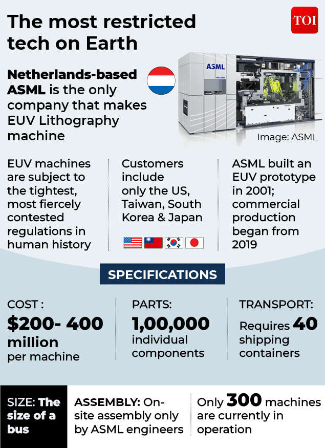
EUV tech is subject to the tightest, most fiercely contested technological regulations in human history.
Because of this structural monopoly, the United States leveraged plurilateral export control frameworks, forcing the Dutch government to block ASML from shipping any EUV systems to Chinese state-backed foundries like SMIC (Semiconductor Manufacturing International Corporation).The Western strategy relied on a simple premise: without ASML, China could never cross the threshold into true sub-5-nanometer chip production.
China’s ‘Manhattan Project ‘
Faced with an existential threat to its tech sector, Beijing did what it always does when backed into a corner: it bypassed market economics and initiated a highly classified, state-directed industrial mobilisation.Coordinated under the oversight of China’s Central Science and Technology Commission and heavily driven by national tech champions like Huawei and the state-backed consortium SiCarrier, China launched its own semiconductor ‘Manhattan Project’ — the US wartime effort to develop the atomic bomb.Six years after launch, the highly classified project achieved a structural shift.In late 2025, inside a heavily fortified, high-security facility in Shenzhen, Chinese engineers successfully activated a functional prototype of an indigenous EUV lithography system.
How Beijing pulled off the impossible
The activation of the working EUV prototype in Shenzhen was a monumental psychological and geopolitical victory for Beijing.It completely shattered the Western dogmatic belief that EUV physics was a barrier China could never overcome on its own.So, how did China manage to bridge a technology gap that experts claimed would take several decades to close?The answer lies in a mix of indigenous scientific breakthroughs and a sophisticated, global shadow procurement network.US intelligence agencies and trade watchdogs have raised alarms over allegations that the components powering the Shenzhen prototype did not all originate from domestic labs.Instead, evidence points to an elaborate “reverse-engineering and refurbishment” scheme.Over the past decade, Chinese entities aggressively stockpiled older-generation ASML DUV tools, as well as secondary equipment from Japanese manufacturers like Nikon and Canon.By utilising front companies, vague secondary markets, and decentralised procurement networks (such as the Shenzhen-based SiCarrier group), China managed to acquire restricted spare parts, alternative sensors, and legacy optical assemblies.The prototype operating in Shenzhen is reportedly a hybrid machine.It combines newly developed Chinese light sources with cannibalised, reverse-engineered components extracted from legitimately purchased legacy systems.US commerce secretary Howard Lutnick recently raised concerns that ASML’s EUV machines may have also reached China in violation of US-led export restrictions. ASML, however, has flatly rejected the possibility.
The human angle
The industrial heist was not just digital or mechanical; it was human.Beijing recognised that blueprints are useless without operational know-how.Reuters reported in December 2025 that the project systematically targeted and poached high-level engineers, system integrators, and software developers directly from ASML’s European hubs and TSMC’s Taiwanese foundries.By offering astronomical compensation packages — sometimes exceeding $700,000 annually along with state-backed security and false operational identities — China imported the exact chemical, mathematical, and mechanical institutional knowledge required to calibrate an EUV system’s 1,00,000 moving parts.
Still a long way to go
Building an early model is a milestone, but mass-producing advanced chips requires industrial‑scale fabs, reliable supply chains for specialised materials, skilled engineers, and years of validated process development.A massive chasm separates a laboratory prototype from a commercial factory floor.
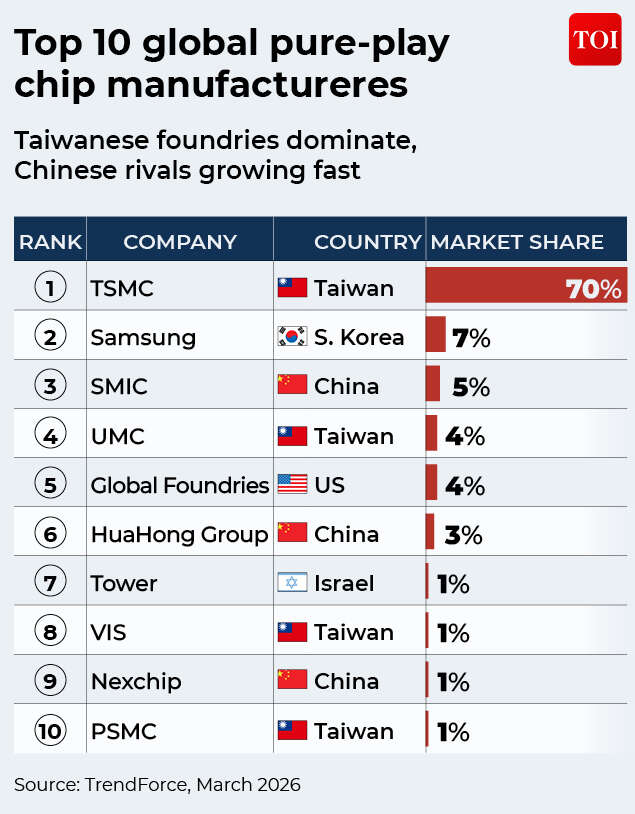
Top 10 chip foundries in the world.
Currently, China’s top chipmaker, SMIC, can produce 7 nm and even rudimentary 5 nm chips, but they do so by forcing older DUV machines through an incredibly inefficient process called quadruple patterning. This involves running a wafer through a DUV machine four separate times to etch a single layer. The downsides are catastrophic for business:
- It drastically lowers the yield rate (the percentage of usable chips per wafer), reportedly keeping it below 50%.
- It drives manufacturing costs up by 40% to 50% compared to TSMC’s EUV-driven processes.
The newly minted Chinese EUV prototype currently generates an output power estimated between 100 and 150 watts, whereas a standard commercial ASML system operates comfortably at 250 to 300 watts to sustain mass production.Consequently, the Chinese tool can currently print only about 40 to 60 wafers per hour, making it commercially unviable for standard market competition.Independent semiconductor analysts suggest that while China has solved the foundational physics of 13.5 nm light generation, mastering production-grade reliability, uptime, mask inspection, and chemical photoresists will take time.The consensus points to 2030 being the realistic threshold for high-volume, commercially viable domestic EUV manufacturing.
The big picture
The revelation of China’s shadow EUV programme underscores a profound truth about technology: when a sovereign superpower considers a piece of technology critical to its national survival, export controls function less like an absolute wall and more like a clock that delays the inevitable.By forcing China’s hand, the West inadvertently triggered the creation of a completely parallel, sanction-proof semiconductor supply chain.The operational prototype in Shenzhen marks the end of a unipolar technological world.Whether or not Beijing can scale this machine to match ASML’s commercial output is secondary to the geopolitical reality: the monopoly has been breached, the secret has been decoded, and the race for total silicon sovereignty is officially wide open.The next decade will decide whether that phase yields secure competition, fractured supply chains, or yet deeper decoupling — with profound consequences for the global balance of economic and military power.